Gallery
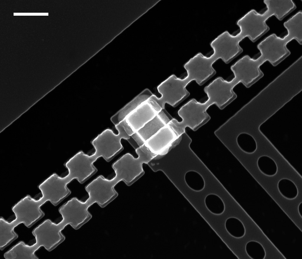
SEM image of piezo-optomechanical quantum transducer between microwave and optical photons (bright box at center: aluminum nitride piezoelectric resonator, nanobeam with ellipses: silicon optomechanical crystal; modulated tethers: aluminum electrodes routed over a phononic bandgap structure; scale bar: 500 nm).

Dark-field optical micrograph of superconducting microwave kinetic inductance resonators patterned in a niobium nitride thin film (scale bar: 10 μm).
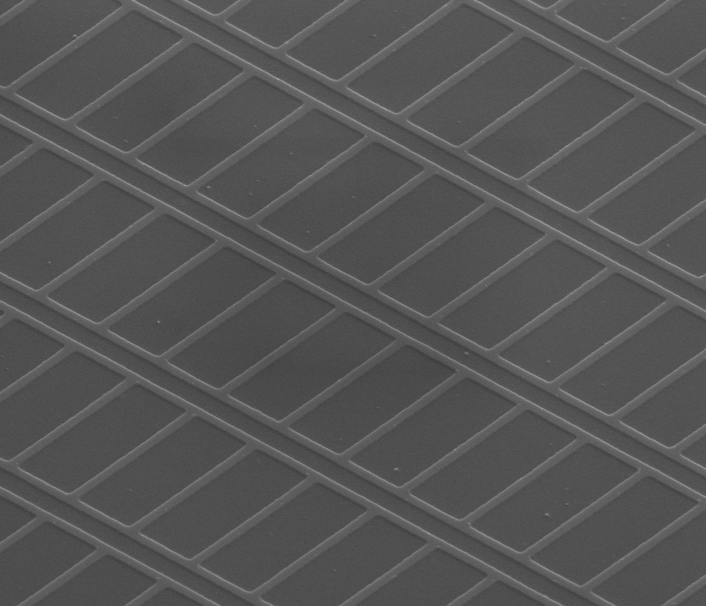
SEM image of superconducting nanowires in the above microwave resonators (wire width: 130nm).
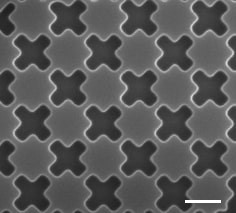
SEM image of a two-dimensional phononic bandgap structure patterned in silicon (scale bar: 300nm).
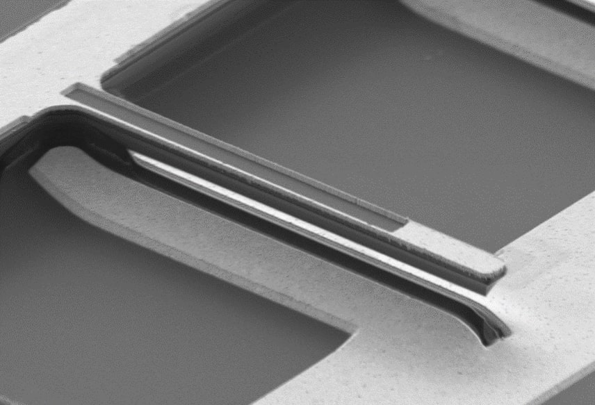
SEM image of a diamond cantilever with surrounding gold electrodes for capacitive actuation (cantilever width: 1 μm).
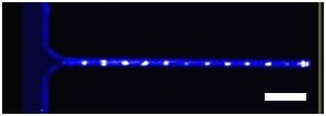
Fluorescence image of an array of silicon-vacancy color-centers in a diamond cantilever (scale bar: 1 μm).
The bizarre and beautiful
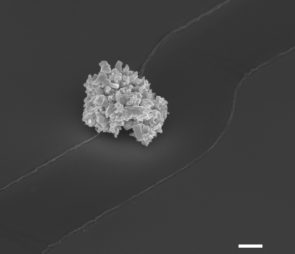
Mystery junk (scale bar: 1 μm).
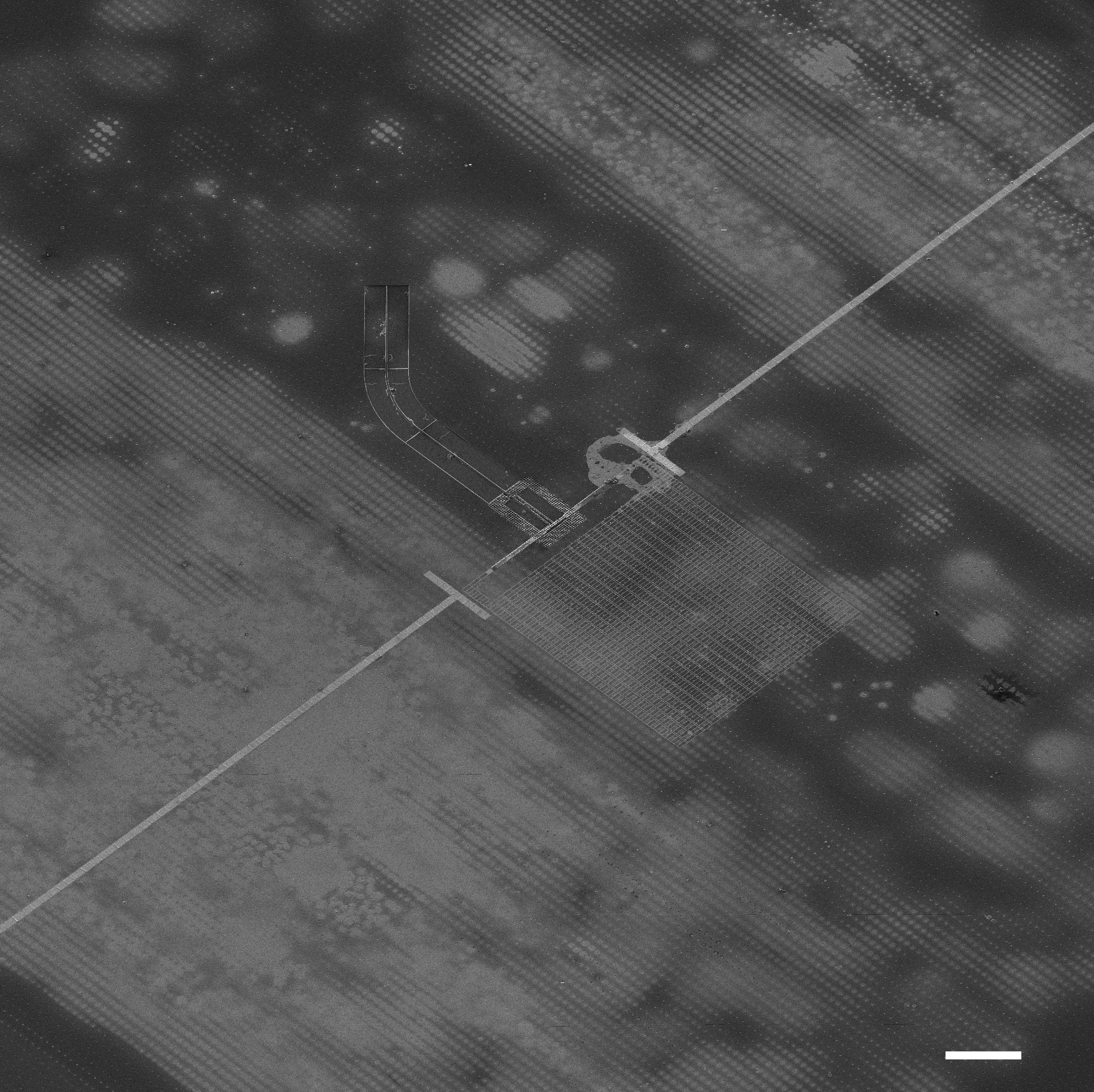
Nano-apocalypse (scale bar: 20 μm).
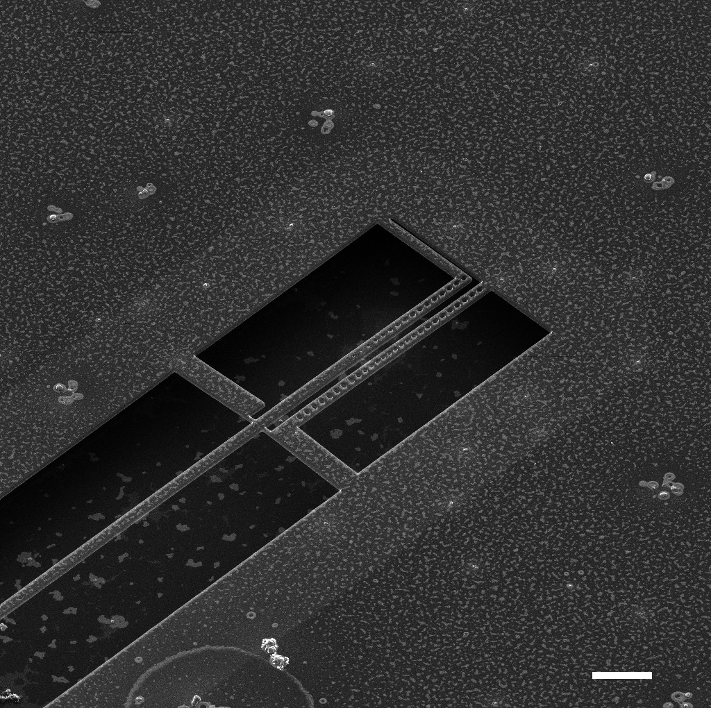
Nano-apocalypse 2 (scale bar: 2 μm).